


Overview
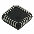
The AD9253BCPZ-125 is a quad, 14-bit analog-to-digital converter (ADC) designed by Analog Devices. It operates at conversion rates of up to 125 million samples per second (MSPS) and is optimized for low cost, low power, small size, and ease of use. The ADC features an on-chip sample-and-hold circuit and requires a single 1.8 V power supply. It is compatible with LVPECL-, CMOS-, and LVDS-compatible sample rate clocks, eliminating the need for external reference or driver components in many applications.
Key Specifications
| Parameter | Value | Unit |
|---|---|---|
| Resolution | 14 | Bits |
| Sampling Rate | 80 MSPS / 105 MSPS / 125 MSPS | MSPS |
| Supply Voltage | 1.8 V | V |
| Power Consumption | 110 mW per channel at 125 MSPS | mW |
| Input Voltage Range | 2 V p-p | V |
| SNR | 74 dB (to Nyquist) | dB |
| SFDR | 90 dBc (to Nyquist) | dBc |
| DNL | ±0.75 LSB (typical) | LSB |
| INL | ±2.0 LSB (typical) | LSB |
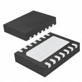
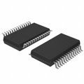
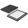
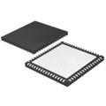
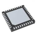
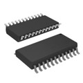
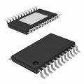
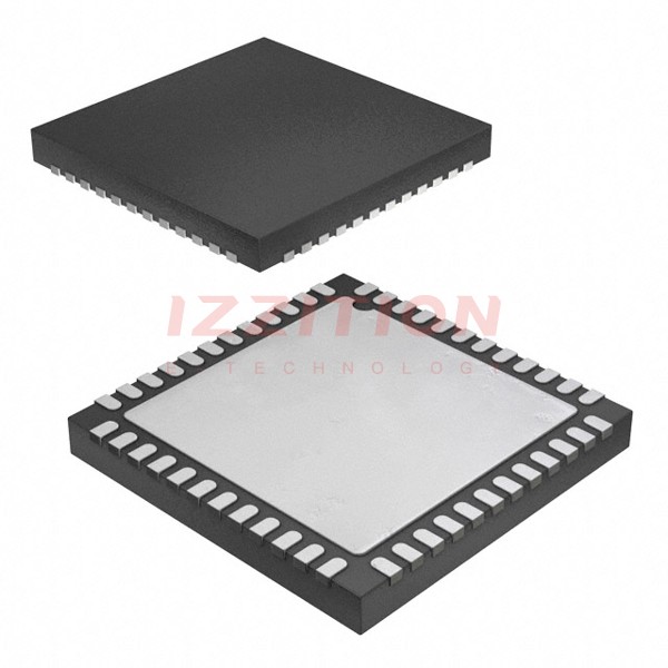
| Package Type | 48-lead LFCSP | |
| Operating Temperature Range | -40°C to +85°C | °C |
Key Features
- Low power operation: 110 mW per channel at 125 MSPS with scalable power options.
- High dynamic performance: SNR = 74 dB and SFDR = 90 dBc (to Nyquist).
- Serial LVDS (ANSI-644, default) and low power, reduced signal option (similar to IEEE 1596.3).
- 650 MHz full power analog bandwidth.
- Programmable output clock and data alignment.
- Built-in and custom digital test pattern generation via SPI interface.
- Full chip and individual channel power-down modes.
- Flexible bit orientation and multichip sync and clock divider.
- RoHS-compliant and specified over the industrial temperature range of -40°C to +85°C.
Applications
- Telecommunications: For precise signal processing in base stations and network equipment, including direct RF downconversion.
- Computing and Data Storage: High-speed data acquisition systems, storage oscilloscopes, and data conversion within large-scale data centers.
- Internet of Things (IoT): Efficient power usage and precise data conversion for sensor data in advanced wearable technologies or smart home devices.
- Medical and High-Speed Imaging: Medical ultrasound, high-speed imaging, and quadrature radio receivers.
- Education and Research: Laboratory equipment such as spectrometers and signal analyzers for advanced experimentation and analysis).
Q & A
- What is the resolution and sampling rate of the AD9253BCPZ-125? The AD9253BCPZ-125 is a 14-bit ADC with sampling rates of up to 125 MSPS.
- What is the power supply requirement for the AD9253BCPZ-125? The ADC requires a single 1.8 V power supply.
- What are the key dynamic performance metrics of the AD9253BCPZ-125? The ADC has an SNR of 74 dB and an SFDR of 90 dBc (to Nyquist).
- What type of output interface does the AD9253BCPZ-125 use? The ADC uses Serial LVDS (ANSI-644, default) and a low power, reduced signal option (similar to IEEE 1596.3).
- What is the input voltage range of the AD9253BCPZ-125? The input voltage range is 2 V p-p.
- Does the AD9253BCPZ-125 support power-down modes? Yes, it supports full chip and individual channel power-down modes.
- What is the operating temperature range of the AD9253BCPZ-125? The operating temperature range is -40°C to +85°C.
- Is the AD9253BCPZ-125 RoHS-compliant? Yes, it is RoHS-compliant).
- What package type is the AD9253BCPZ-125 available in? It is available in a 48-lead LFCSP package).
- What are some potential applications of the AD9253BCPZ-125? It can be used in telecommunications, computing and data storage, IoT devices, medical and high-speed imaging, and education and research).